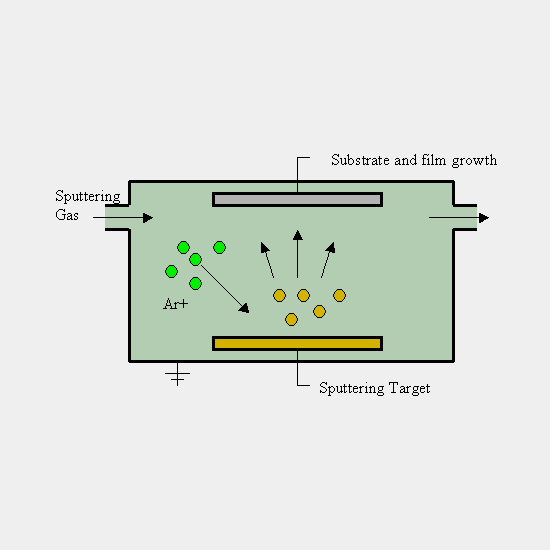
Sputtering is a process used in the field of thin-film deposition, commonly employed in semiconductor manufacturing, optics, and materials science. It involves the removal of atoms or molecules from a solid target material and depositing them onto a substrate to create a thin film. This process is primarily driven by bombarding the target material with high-energy ions, typically from a plasma or gas discharge. As these ions collide with the target, they transfer energy to the target atoms, causing them to be ejected from the surface and deposited onto a substrate, creating a thin film.
Types of Sputtering Techniques:
There are several types of sputtering techniques, each tailored for specific sputtering applications. Common methods include DC sputtering, RF sputtering, and magnetron sputtering, which use different power sources and magnetic fields to enhance deposition. These techniques allow precise control over film thickness, composition, and uniformity.
- DC Sputtering: In this method, a direct current (DC) voltage is applied between the target material and the substrate. The target serves as the cathode, while the substrate is the anode. Argon gas is often used as the sputtering gas.
- RF Sputtering: Radio-frequency (RF) sputtering involves applying an RF power source to create a plasma in the sputtering chamber. This plasma generates high-energy ions, which sputter the target material.
- Magnetron Sputtering: This is a variant of DC or RF sputtering that uses magnets to enhance the process. The magnetic field confines electrons and increases their mobility, leading to higher plasma density and more efficient sputtering.
- Reactive Sputtering: In reactive sputtering, a reactive gas, such as nitrogen or oxygen, is introduced into the sputtering chamber along with the inert gas (usually argon). The target material reacts with the reactive gas, leading to the deposition of compounds on the substrate.
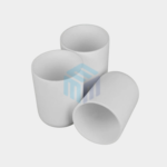
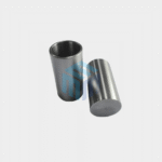
Sputtering targets are the materials that are used as the source for thin-film deposition in the sputtering process. The choice of sputtering target material depends on the desired properties of the thin film and its intended application.
Sputtering Target Materials:
Sputtering target materials range from pure metals like gold, silver, and titanium to complex alloys and ceramics. The choice of target directly influences the properties of the deposited thin film. Selecting the right material ensures optimal performance for applications in electronics, optics, and protective coatings.
Some common sputtering target materials include:
- Metals: Metals like aluminum, copper, gold, silver, and titanium are frequently used for sputtering applications where electrical conductivity or metal coatings are required.
- Semiconductors: Materials like silicon, indium tin oxide (ITO), and gallium arsenide are used for semiconductor device fabrication.
- Dielectrics: Dielectric materials like silicon dioxide (SiO2), silicon nitride (Si3N4), and aluminum oxide (Al2O3) are used for insulating layers and optical coatings.
- Compound Materials: Complex materials, such as oxides, nitrides, and carbides, can be sputtered to create specific properties or compound thin films, e.g., magnetron sputtering of iron oxide for magnetic applications.
- Ceramics: Materials like alumina (Al2O3) and zirconia (ZrO2) can be used for applications requiring hardness, wear resistance, or thermal insulation.
- Superconductors: High-temperature superconducting materials like yttrium barium copper oxide (YBCO) are used for specific research and device applications.
The choice of sputtering target material is essential to control the composition, structure, and properties of the deposited thin film. Researchers and manufacturers carefully select the appropriate target material to meet the requirements of their specific applications.
Common Target Materials and Their Applications
Sputtering targets come in a wide range of materials, each suited for specific industries:
-
Metals: Aluminum (Al) for reflective coatings, Copper (Cu) for interconnects, Titanium (Ti) for adhesion layers, Gold (Au) and Silver (Ag) for high-conductivity and decorative films.
-
Semiconductors: Silicon (Si) for microelectronics, Indium Tin Oxide (ITO) for transparent conductive films, Gallium Arsenide (GaAs) for optoelectronic devices.
-
Dielectrics: Silicon Dioxide (SiO₂), Silicon Nitride (Si₃N₄), and Aluminum Oxide (Al₂O₃) for insulation, passivation, and barrier layers.
-
Ceramics and Compounds: Nitrides, carbides, and oxides for wear resistance, hardness, and specialized functional coatings.
-
Superconductors: Yttrium Barium Copper Oxide (YBCO) for high-performance electronic applications.
Why Your Target Material Matters
The sputtering target is more than just a raw material—it defines the chemical, physical, and structural characteristics of the deposited film. Choosing the wrong target can lead to issues like poor adhesion, non-uniform coating, reduced conductivity, or suboptimal optical performance. For instance, in semiconductor fabrication, a high-purity target ensures defect-free layers, while in optics, the right dielectric material prevents unwanted light absorption. Material purity, density, and grain structure all influence coating quality, making target selection a critical engineering decision.
In conclusion, sputtering is a versatile thin film deposition technique widely used across industries for its precision and adaptability. By choosing from a broad range of sputtering targets—metals, alloys, and ceramics—manufacturers can tailor coatings to meet specific electrical, optical, or protective requirements, driving innovation in modern technology.
Applications: Where Sputtering Shines
Sputtering plays a vital role across numerous high-tech and industrial applications:
-
Semiconductors & Microelectronics – For depositing conductive, insulating, and barrier layers in integrated circuits.
-
Optical Coatings – For anti-reflective layers, mirrors, and decorative finishes.
-
Solar Energy – For thin-film photovoltaic cells, improving efficiency and durability.
-
Aerospace & Defense – For thermal barrier coatings and protective films.
-
Medical Devices – For biocompatible coatings on implants and surgical tools.
-
Hard & Wear-Resistant Films – For tooling, machinery components, and cutting instruments.
M-Kube Enterprise is an Australian company catering customized laboratory products, laboratory consumables and laboratory solutions in Australia, New Zealand, Singapore, Malaysia, South Korea, India, Dubai, Philippines, Indonesia and Vietnam.
Conclusion: The Role of Sputtering in Modern Technology
From microchips to spacecraft, sputtering enables the creation of precisely engineered thin films that drive innovation across industries. Its ability to deposit complex materials with high purity and accuracy ensures it remains a preferred method for advanced manufacturing. With the right sputtering targets and process parameters, engineers can achieve coatings that meet the most demanding mechanical, optical, and electrical specifications—cementing sputtering’s place at the forefront of material science and technology.