Sputtering has become one of the most widely used and versatile thin-film deposition methods, playing a pivotal role in shaping today’s high-tech world. By bombarding a target material with energetic ions, sputtering enables the precise formation of ultra-thin, uniform coatings on a wide range of substrates. This technique offers exceptional control over film thickness and composition, making it indispensable for industries that demand performance and precision — from semiconductor manufacturing and solar energy to advanced optics and hard protective coatings.
Sputtering techniques offer several advantages and have a wide range of applications in various industries and research fields. Some of the key advantages and applications of sputtering techniques include:
Advantages of Sputtering Techniques
Sputtering techniques offer outstanding advantages, including precise control over film thickness and composition, excellent adhesion to diverse substrates, and the ability to deposit a wide range of materials. This makes them ideal for producing uniform, high-quality coatings essential in electronics, optics, and protective applications.
- Precise Thin-Film Deposition: Sputtering allows for precise control over the thickness and composition of thin films, making it suitable for applications where accuracy and uniformity are crucial.
- High Purity and Clean Deposition: Sputtering produces high-purity films with minimal impurities, making it suitable for applications where contamination is a concern.
- Versatility: Sputtering can deposit a wide range of materials, including metals, semiconductors, insulators, and compound materials, enabling diverse applications.
- Excellent Adhesion: Sputter-deposited films typically exhibit excellent adhesion to substrates, reducing the risk of delamination.
- Wide Range of Substrates: Sputtering can be used on various substrate materials, including silicon wafers, glass, plastics, and even temperature-sensitive materials.
- Reactive Sputtering: Reactive sputtering allows for the deposition of compounds and complex materials, expanding its utility in applications requiring specific material properties.
- Tunable Properties: By adjusting process parameters and target materials, sputtering can tailor the properties of thin films, such as electrical conductivity, optical characteristics, and mechanical properties.
These advantages make sputtering an indispensable choice for industries that demand precision, durability, and consistent quality. By leveraging its unique benefits, manufacturers can create cutting-edge products that perform reliably even in the most demanding environments.
Advantages of Sputtering for Thin Film Deposition
Sputtering is widely used for thin film deposition because it produces uniform, high-quality coatings with excellent adhesion and precise thickness control. The process is suitable for depositing metals, ceramics, semiconductors, and compound materials on various substrates.
Key advantages of sputtering include:
- High film uniformity and thickness control
- Excellent coating adhesion
- Low contamination levels
- Compatibility with a wide range of materials
- Ability to deposit complex and high-purity films
These benefits make sputtering ideal for electronics, optics, energy, and advanced coating applications.
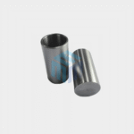
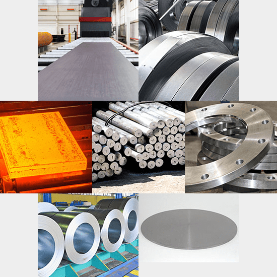
Common Sputtering Target Materials
The choice of sputtering target material determines the composition and properties of the deposited thin film.
Metals
Common metallic targets include aluminum (Al), copper (Cu), titanium (Ti), gold (Au), and silver (Ag), used in conductive coatings and semiconductor devices.
Ceramics
Ceramic targets such as alumina (Al₂O₃) and zirconia (ZrO₂) are used for wear-resistant, insulating, and protective coatings.
Semiconductors
Materials like silicon (Si), indium tin oxide (ITO), and gallium arsenide (GaAs) are widely used in electronics and optoelectronic applications.
Compound Targets
Oxides, nitrides, and carbides are used to produce specialized functional coatings with improved hardness, conductivity, or optical performance.
Applications of Sputtering Techniques
Sputtering techniques are widely used to create thin films for semiconductors, solar cells, optical coatings, and hard protective layers. They enable precise fabrication of microelectronic circuits, anti-reflective and decorative surfaces, and wear-resistant components. This versatility makes sputtering essential across electronics, energy and medical industries.
- Semiconductor Fabrication: Sputtering is widely used in the semiconductor industry to deposit thin films of metals, dielectrics, and semiconductors for integrated circuits, photovoltaic cells, and microelectromechanical systems (MEMS) devices.
- Optical Coatings: Sputtering is used to create anti-reflective coatings, optical filters, and mirrors with precise optical properties in applications like lenses, displays, and mirrors.
- Data Storage: Sputtering is employed in the manufacture of hard disk drives, where thin-film magnetic materials are deposited for data storage and read/write heads.
- Solar Cells: Sputtering is utilized to deposit thin-film photovoltaic materials, such as cadmium telluride (CdTe) and copper indium gallium selenide (CIGS), for solar cell production.
- Thin-Film Electronics: It is used in the production of thin-film transistors (TFTs) for flexible displays, OLEDs, and electronic paper.
- Wear-Resistant Coatings: Sputtered thin films are used to enhance the hardness, wear resistance, and lubricity of cutting tools, bearings, and other mechanical components.
- Decorative Coatings: Sputtering can be employed to deposit decorative coatings on jewelry, watch dials, and other items to achieve various colors and finishes.
- Magnetic Recording Media: Thin-film magnetic materials deposited through sputtering are used in magnetic tapes and data storage applications.
- .Sensors: Sputtering is used in the fabrication of various sensors, including gas sensors, pressure sensors, and biosensors, due to its ability to deposit precise, thin-film materials.
- Barrier Coatings: Sputtered materials are used to create barrier layers in packaging materials to protect against moisture and gas penetration.
- MEMS and Microfabrication: Sputtering is used in the fabrication of microelectromechanical systems (MEMS) and microdevices for a wide range of applications, from accelerometers to inkjet nozzles.
- Research and Development: Sputtering techniques are valuable tools in materials science and academic research for exploring novel materials and their properties.
Overall, sputtering techniques are versatile and find applications in numerous industries, from electronics and optics to automotive, contributing to the development of advanced materials and technologies.
In conclusion, the wide-ranging applications of sputtering techniques highlight their crucial role in advancing modern technology. From enhancing electronic devices and solar panels to improving optical components and protective surfaces, sputtering continues to drive innovation across countless industries. Its versatility and precision ensure it remains a cornerstone process for creating high-performance, reliable products well into the future.
M-Kube Enterprise is an Australian company catering customized laboratory products, laboratory consumables and laboratory solutions in Australia, New Zealand, Singapore, Malaysia, South Korea, India, Dubai, Philippines, Indonesia and Vietnam.